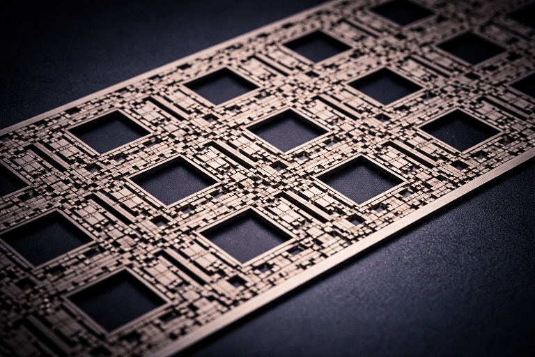
Precision stamped metal components manufactured for semiconductor lead frames and electronic applications with fine pitch control, burr management, and stable reel-to-reel strip performance at production scale.
Progressive stamping capability with controlled edge quality and stable strip handling for high-density electronic components.
Representative stamped component structures developed for high-precision electronics programs.
Our precision metal stamping capability supports high-density electronic component manufacturing through controlled Korean tooling design, material handling, and process stability.
These components represent established engineering capability developed through Korean precision systems — supporting semiconductor lead frame and insert molded electronic component programs — and proven across multiple program types.
As a precision stamping manufacturer, Moldrite supports OEM and OSAT programs requiring high-density lead frames, stamped metal components, and reel-to-reel processed electronic parts for semiconductor and electronics applications.
Capability includes fine pitch tolerance down to ±0.013mm with burr control in the range of 0.001–0.005mm, enabling high-density lead frame and electronic component manufacturing.
Requirements defined
Korean engineering
Performance verified
Established systems
Structured pathway
Integrated stamping process including progressive die design, reel-to-reel strip processing, plating integration, and inspection for high-reliability electronic components.
Precision stamped components are manufactured for OEM and OSAT programs requiring high-density lead frames, fine-pitch electronic parts, and reel-to-reel processed metal components across global semiconductor and electronics supply chains.
For precision electronics and semiconductor component programs.
Share Your RequirementFor injection molding: Moldrite India →